Continuous-Time Latch Family
A1210, A1211,
A1212, A1213,
and A1214
10
Allegro MicroSystems, LLC
115 Northeast Cutoff
Worcester, Massachusetts 01615-0036 U.S.A.
1.508.853.5000; www.allegromicro.com
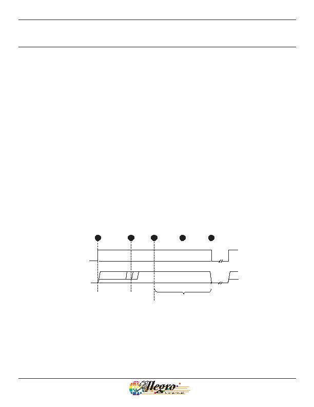
Figure 2. Continuous-Time Application, B < B
RP
.. This figure illustrates the use of a quick cycle for chopping V
CC
in order to conserve battery power.
Position 1, power is applied to the device. Position 2, the output assumes the correct state at a time prior to the maximum Power-On Time, t
PO(max)
.
The case shown is where the correct output state is HIGH
. Position 3, t
PO(max)
has elapsed. The device output is valid. Position 4, after the output is
valid, a control unit reads the output. Position 5, power is removed from the device.
V
CC
V
OUT
Output Sampled
1
5
4
2
t
t
t
PO(max)
3
ADDITIONAL APPLICATIONS INFORMATION
Extensive applications information for Hall-effect devices is
available in:
" Hall-Effect IC Applications Guide, Application Note 27701
" Hall-Effect Devices: Gluing, Potting, Encapsulating, Lead
Welding and Lead Forming, Application Note 27703.1
" Soldering Methods for Allegros Products SMT and Through-
Hole, Application Note 26009
All are provided in Allegro Electronic Data Book, AMS-702,
and the Allegro Web site, www.allegromicro.com.
发布紧急采购,3分钟左右您将得到回复。
相关PDF资料
A1220LUA-T
IC HALL EFFECT LATCH 3V 3-SIP
A1242LUA-I2-T
IC LATCH HALL EFFECT 3-SIP
A1244LUA-I2-T
IC HALL EFFECT LATCH SIP-3
A1302KUA-T
IC SENSOR HALL EFFECT 3-SIP
A1323LLHLT-T
IC SENSOR HALL EFFECT SOT23W
A1351LKTTN-T
IC SENSOR HALL EFFECT 4-SIP
A1354KKT-T
IC SENSOR HALL EFFECT 4-SIP
A1356LKB-T
IC SENSOR HALL EFFECT 3 SIP
相关代理商/技术参数
A1212
制造商:M/A-COM Technology Solutions 功能描述:RF AMP CHIP SGL CASCADABLE AMP 1.2GHZ 8V 4PIN TO-8 - Bulk 制造商:M/A-COM Technology Solutions 功能描述:GAIN BLOCK
A1212_1
制造商:MA-COM 制造商全称:M/A-COM Technology Solutions, Inc. 功能描述:Cascadable Amplifier 100 to 1200 MHz
A1212116RT
制造商:Pentair Technical Products / Hoffman 功能描述:12x12x116 3R Wire Trough
A1212120T1T
制造商:Pentair Technical Products / Hoffman 功能描述:12X12 120 LNG TYPE 1 TROUGH
A121212GSC
制造商:Pentair Technical Products / Hoffman 功能描述:Galvanized Box, Screw Cover
A121224RT
制造商:Pentair Technical Products / Hoffman 功能描述:Wire Trough, Type 3R , 12.00x12.00x24.00, Steel
A-121224RT
制造商:Pentair Technical Products / Hoffman 功能描述:Wire Trough, Type 3R
A121224T1T
制造商:Pentair Technical Products / Hoffman 功能描述:12X12 24 L0NG TYPE 1 TROUGH